Inverter Analysis and Design
This current depends on the gate-to-source voltage, vGS, which is the same as vIN, and the drain-to-source voltage, vDS, which is the same as vOUT. With vIN less than VT, the pull-down current is
This current depends on the gate-to-source voltage, vGS, which is the same as vIN, and the drain-to-source voltage, vDS, which is the same as vOUT. With vIN less than VT, the pull-down current is
In this article, let''s embark on a comprehensive journey to unravel the mysteries surrounding inverter voltage, exploring its nuances, applications, and the Tycorun inverter''s unique
We can instead have a PWM scheme that treats each half-bridge equally, operating at a frequency fsw with output voltage Vx and VL seeing ripple centered near Z · fsw and its harmonics.

It is important to notice that the CMOS does not contain any resistors, which makes it more power efficient that a regular resistor-MOSFET inverter. As the voltage at the input of the CMOS device

V OH and V OL represent the “high” and “low” output voltages of the inverter V = output voltage when OH Vin = ''0'' (V Output High) V = output voltage when OL Vin = ''1'' (V Output Low) Ideally, V = Vdd
Inverter Voltage Transfer Characteristics Output High Voltage, V OH maximum output voltage occurs when input is low (Vin = 0V) pMOS is ON, nMOS is OFF pMOS pulls Vout to VDD V OH = VDD

Derive expressions for Static, Dynamic and Short Circuit power of an inverter. Rise delay. Output goes from L ↑ H - tpLH. Fall delay . Output goes from H ↓ L - tpHL. Rising propagation delay should be
VIL is the input low voltage which corresponds to an output high voltage with a slope of -1. the most common type of inverter in VLSI is CMOS. This is due to the low static power consumption. BUT, we
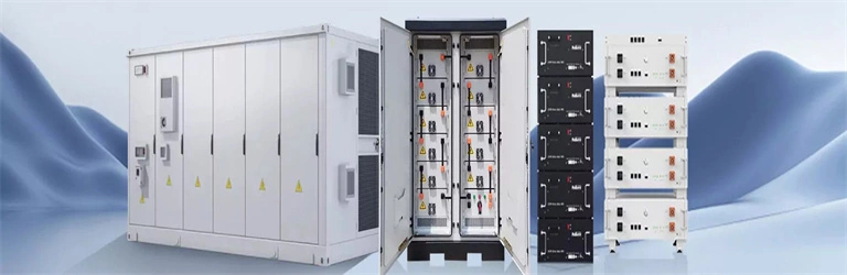
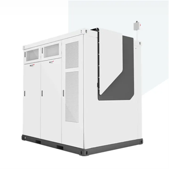
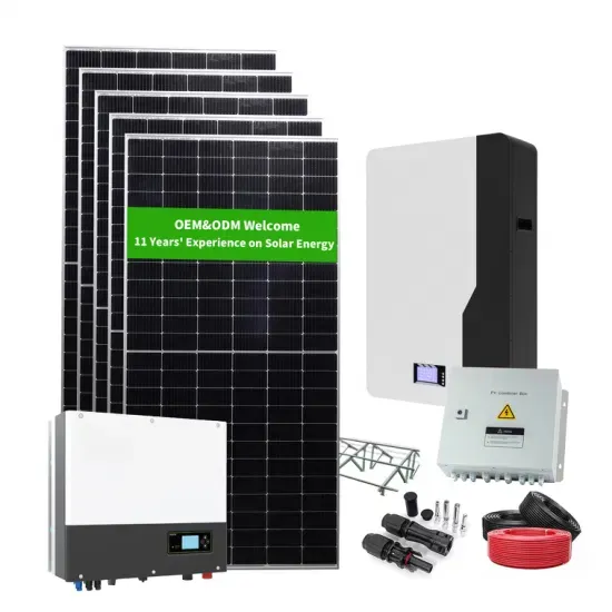
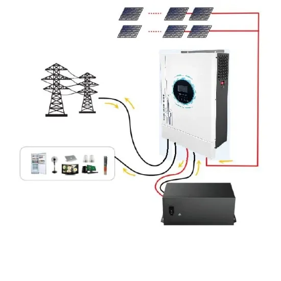
Each inverter comes with a voltage range that allows it to track the maximum power of the PV array. It is recommended to match that range when selecting the inverter and the PV array parameters.
From the given figure, we can see that the input voltage of inverter is equal to the gate to source voltage of nMOS transistor and output voltage of inverter is equal to drain to source voltage of nMOS transistor.
PDF version includes complete article with source references. Suitable for printing and offline reading.